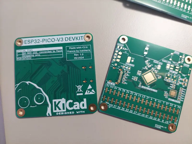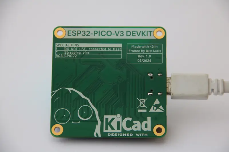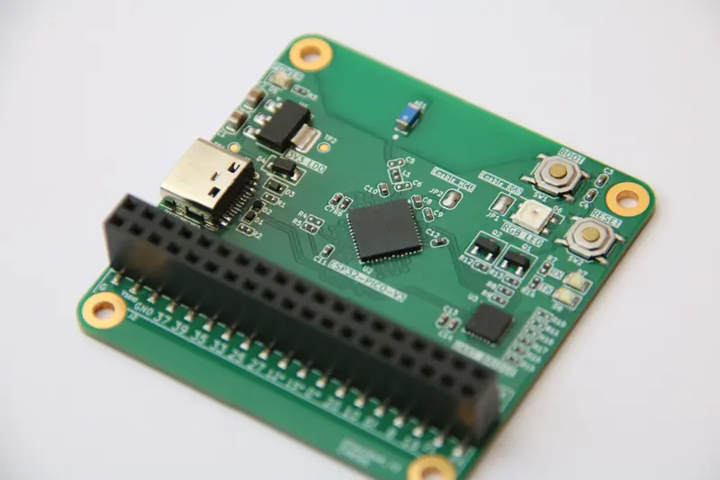
ESP32 Pico V3 Development Kit
First successful PCB design - ESP32 development board featuring the ESP32 Pico V3 chip.
First successful PCB design - ESP32 development board featuring the ESP32 Pico V3 chip.
This development board was my first successful PCB design, created as a stepping stone for a larger project that required the ESP32 Pico V3 chip. Rather than dive directly into a complex design, I decided to first master the fundamentals with a simpler board that would also serve as a useful development tool.
The ESP32 Pico V3’s compact form factor and integrated wireless capabilities made it ideal for the target application, but its fine-pitch QFN package (0.5mm pitch) and RF requirements meant I needed to understand proper PCB design practices before attempting anything more ambitious.
The primary objective was to create a reliable development platform while learning essential skills: RF design and antenna placement, power supply design for wireless transmission, mixed-signal PCB layout, and professional SMD assembly techniques using stencil printing and reflow soldering.
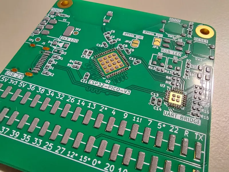
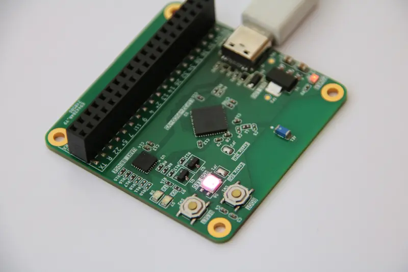
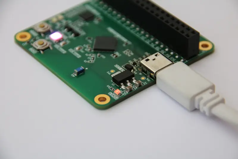
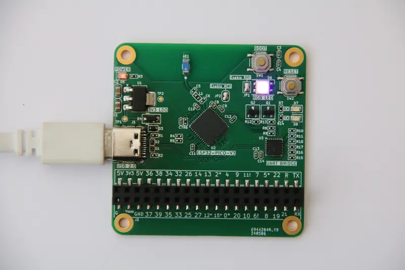
The board provides complete access to all ESP32 Pico V3 pins through standard 2.54mm headers, integrated USB programming via CP2102N bridge, and proper RF design with chip antenna implementation. It functioned correctly on first power-up and has since served as a reliable development platform for multiple projects.
Complete design decisions, assembly methodology, and troubleshooting process are documented in the development journal.
Successfully implemented chip antenna design following Espressif’s application notes and reference designs. This was my first experience with RF layout, requiring careful attention to ground plane requirements, impedance matching, and keepout zones around the antenna area.
The antenna design worked on first attempt, demonstrating that careful adherence to manufacturer guidelines and reference designs yields reliable results even without prior RF experience. This gave me confidence to include wireless functionality in future projects.
Developed stable 3.3V power delivery with appropriate decoupling capacitors and filtering, learning to account for the ESP32’s dynamic power requirements during wireless transmission. The power supply design followed industry best practices with bulk capacitance near the power input and smaller decoupling caps close to the IC.
Understanding power supply stability proved essential - wireless modules can have significant current spikes during transmission that require proper capacitor selection and placement to prevent voltage droops and instability.
Learned to route a PCB with both digital GPIO and RF sections, understanding signal integrity considerations and the importance of proper ground plane usage. The layout process taught me about trace impedance, return paths, and minimizing coupling between different circuit sections.
The board layout prioritizes functionality and reliability while maintaining compact dimensions suitable for prototyping. All GPIO pins are accessible through standard 2.54mm headers, making it easy to integrate into breadboard-based projects.
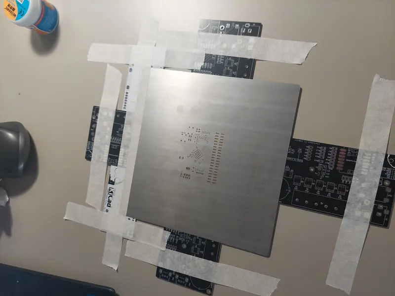
Gained hands-on experience with professional assembly techniques using laser-cut stencil for solder paste application and hotplate reflow soldering. Previous boards were a mix of through-hole and large SMD components (0805), so this was my first time properly using solder paste with a stencil and doing a complete SMD board with fine-pitch QFN (0.5mm pitch) components.
The reflow process using a simple hotplate worked well for the small board size. These assembly skills proved invaluable for subsequent projects with even finer-pitch components.