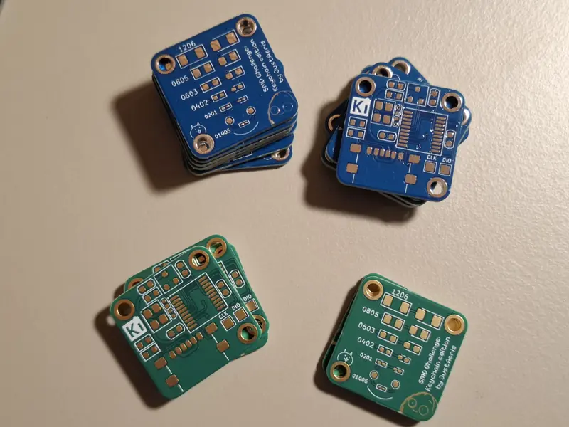
SMD Challenge: Keyring Edition
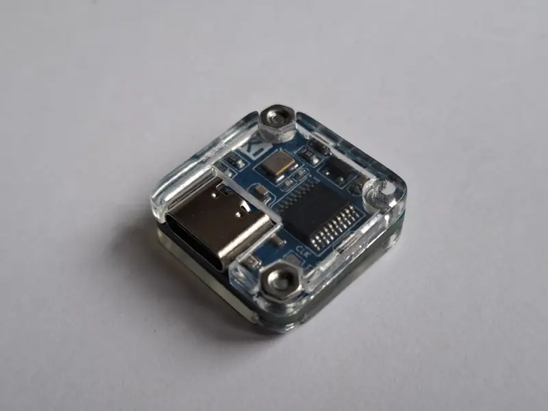
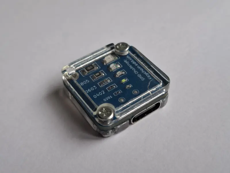
Portable keychain featuring hand-soldered SMD components from 1206 down to 01005, with transparent protective enclosure
Portable keychain featuring hand-soldered SMD components from 1206 down to 01005, with transparent protective enclosure
This project reimagines the popular SMD Challenge by MakersBox as a portable keychain, creating a practical demonstration of advanced hand-soldering that can be carried daily rather than remaining on a workbench.
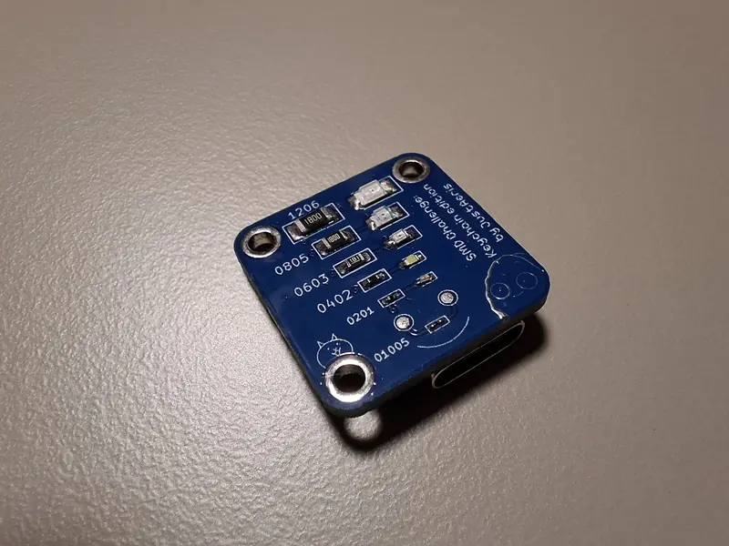
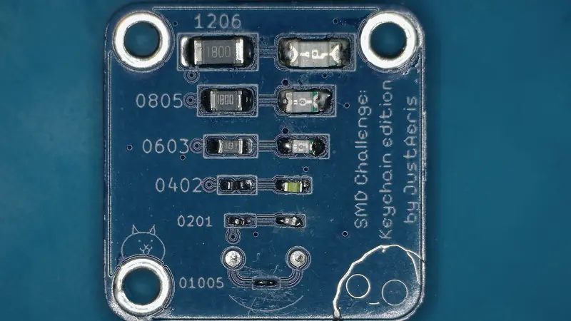
The design features an STM32F030F4Px microcontroller with progressive component sizes from 1206 down to 01005 (0.4×0.2mm), creating a structured challenge for precision soldering skill development.
Key technical decisions include full USB-C compatibility with proper CC resistor configuration, custom transparent enclosure for protection while maintaining visibility, and adaptive PWM brightness control to handle unexpectedly bright LEDs.
The completed device functions as a 20×20×7.5mm keychain with six LED animation sequences, 39mA peak consumption, and reliable daily carry durability. Complete design decisions, assembly methodology, and troubleshooting process are documented in the development journal.
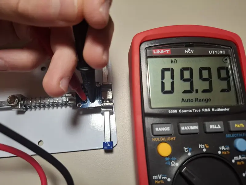
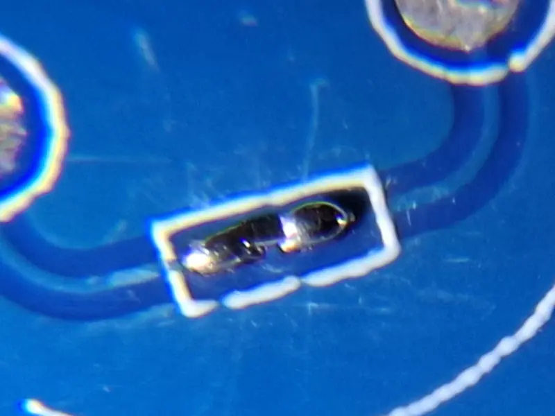
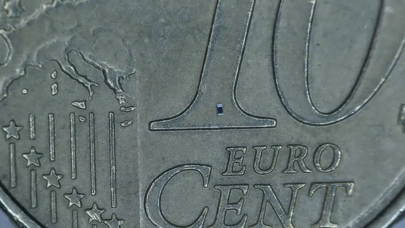
Successfully hand-soldered 0.4×0.2mm (01005) resistor at 23× magnification. Component measures correctly at 10kΩ, confirming reliable electrical connection despite being at the practical limit of hand assembly. Lost half a day when first attempt damaged a pad.
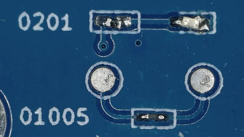
Blue LEDs significantly brighter than expected. Rather than redesigning the PCB, implemented hardware PWM using Timer 14 for the 0201 LED and software PWM for the 0402 LED. Demonstrated adaptive problem-solving while highlighting the importance of thorough LED characterization in design phase.
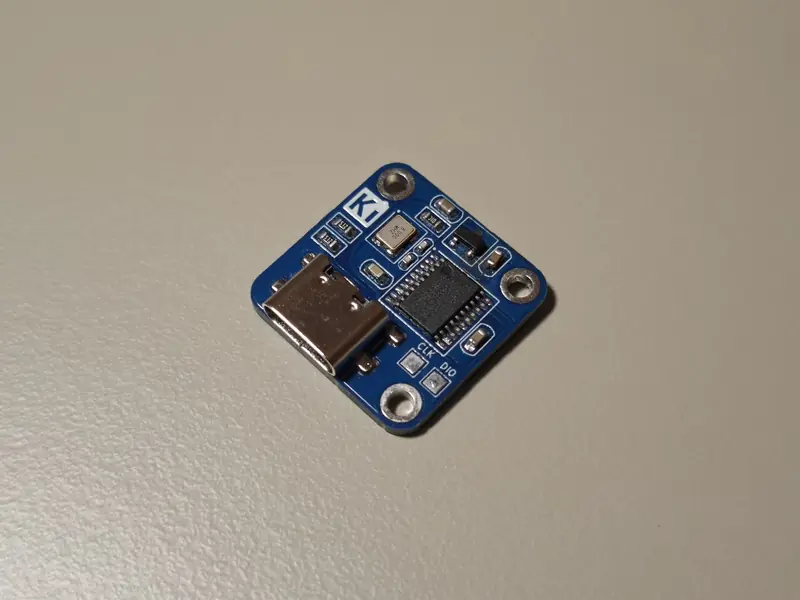
Full USB-C compliance with 5.1kΩ CC resistors enabling USB-C to USB-C operation. XC6206P332MR LDO regulator provides stable 3V3 power with measured 39mA peak current consumption during LED animations. Clean power delivery despite miniaturized layout.
Two-piece transparent SLA-printed enclosure maintains component visibility while providing protection. Flush M2 screws prevent snagging, 7.5mm total thickness suitable for keychain use. Internal clearances accommodate solder joints and component tolerances without requiring perfect assembly precision.
The complete PDF documentation includes detailed technical diagrams, full circuit schematics, design decisions, testing procedures, and troubleshooting guides.
View Full Documentation